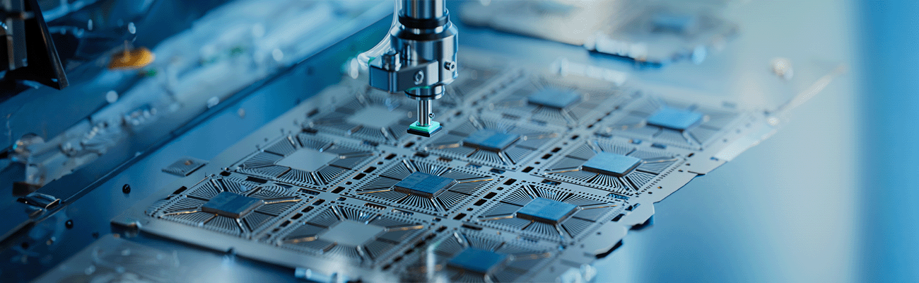
The impact of moisture on semiconductor manufacturing
Water may be the basis of all life, but when it comes to specialized processes such as semiconductor manufacturing, it’s usually one of the last compounds you want around.
The presence of water vapor can have very significant implications, not just on the technical front but also for business outcomes. Even minimal amounts of water vapor can introduce impurities or lead to oxidation on wafer surfaces, creating defects that adversely affect the electrical characteristics of semiconductor devices.
This can result in reduced production efficiency, increased production costs, and extended manufacturing times, directly impacting profitability and market competitiveness.
Precise control of humidity and water vapor during critical processes like lithography, deposition, and etching is essential to maintain the structural integrity of semiconductor layers and achieve the desired product quality. Effective management of water vapor is not only crucial for upholding the high performance standards and reliability demanded by semiconductor devices but also for ensuring efficient production processes, minimizing waste, and maintaining a strong competitive position in the market.
Moisture contamination in chemical vapor deposition
Chemical Vapor Deposition (CVD) is a widely used technique in the semiconductor industry. It involves the chemical reaction of gas-phase precursors that decompose or react on a substrate surface to produce a solid material, forming thin films or coatings.
Moisture contamination directly affects the purity and integrity of deposited films. Even minimal moisture levels can introduce unwanted hydroxyl groups or catalyze oxidation on the substrate, leading to defects in the film that negatively impact device performance. Such defects can lead to electrical instabilities, diminished dielectric strength, or alterations in refractive indices, severely compromising the functionality of semiconductor devices.
To address these challenges, it is critical to implement comprehensive moisture control and mitigation strategies within CVD processes.
Key tactics include the use of rigorous dry gas purging, advanced vacuum systems, and the integration of desiccants to eliminate moisture. Additionally, using chilled mirror hygrometers allows for accurate monitoring and control of moisture within the CVD environment. This combination of strategies is essential for ensuring the deposition of high-quality films that meet the exacting standards necessary for semiconductor device production.
Moisture contamination in plasma etching
Selective etching, typically following the photolithography stage, is crucial for creating the precise sub-micron shapes and patterns essential for circuit design. The process involves the use of etchant gases, specifically fully fluorinated compounds (FFCs), which are activated in argon plasmas above the wafer substrate. These gases engage in a selective reaction with specific materials on the semiconductor wafer, meticulously carving out the complex circuit patterns needed for the device's functionality.
Moisture presence can significantly impact plasma formation and, consequently, the etching quality. As a result, it is considered best practice to continuously monitor the moisture content in the FFCs before their introduction into the etcher or CVD chamber.
Moreover, plasma gases, including halides and nitrogen trifluoride, are also used for chamber cleaning. However, even trace levels of moisture can compromise plasma quality and the efficiency of the cleaning process. Close monitoring of moisture levels is, therefore, essential to maintain the integrity of both the etching and cleaning phases, ensuring high-quality production outcomes.
Moisture measurement instruments for semiconductor manufacturing
Help is at hand.
PST offers a number of advanced sensors and analyzers for measuring moisture at all key stages of the semiconductor manufacturing process. These include dew-point transmitters, such as our latest Easidew EA2 capable of detecting dew point between -110 and +20 oCdp, with an accuracy of ±2 oCdp, and our QMA401, which uses a quartz crystal microbalance that gives a sensitivity of just 0.1 ppmV, making it ideal for use in CVD and etching chambers.
Our newest product is the S8000 RS – a fully automated chilled mirror hygrometer, designed to improve the speed, precision and flexibility of trace moisture measurement under demanding conditions.
The S8000 RS delivers exceptional precision, maintaining an accuracy of ±0.1 oC at temperatures reaching down to -90 oCfp. It demonstrates excellent stability and reproducibility, with a minimal variation of ±0.05 oCdp at -90 oCfp, which further tightens to ±0.025 oCdp at -80 oCfp.
The accuracy of the device is significantly enhanced through the use of a sophisticated gold-plated copper mirror. This, along with precise cooling and Dynamic Contamination Correction, ensures the formation of a consistent condensate layer, facilitating accurate and reliable measurements.
Our latest hygrometer model is equipped with various communication options, including Modbus RTU through USB, TCP/IP, and 4…20 mA interfaces, alongside internal data-logging capabilities directly to a standard SD card. As with every product we offer, the S8000 RS is supported by a comprehensive suite of technical support and after-sales services, ensuring our customers have access to the necessary assistance for optimal performance.
Read more about moisture and oxygen measurement in semiconductor manufacturing.
With 50 years’ experience in the development of moisture, humidity and dew-point technology, we are the application experts for all trace moisture and hydrocarbon measurement applications. If you would like to discuss your requirements, please contact our team today.
Gases used in semiconductor manufacturing are normally classified as either ‘bulk gases’ or ‘electronic special gases’ (ESGs); these include nitrogen, oxygen, argon, helium, hydrogen and carbon dioxide. There are over a hundred ESGs, produced in both pure and blended formats, with typical examples including hexafluoroethane (C2F6), octafluorocyclobutane (C4F8) and germane (GeH4).
Nitrogen is probably the most widely used gas in the semiconductor industry. As a result, many manufacturers now use on-site nitrogen generation systems. These also use moisture measurement sensors, which are fitted to the outlet of drying chambers, both to monitor the purity of the gas before it is used for subsequent process duties and to control the energy efficiency of the dryers themselves.
Related Categories
Precision Chilled Mirror Reference Hygrometers
Related Information
Related Blogs
How to Ensure Quality in OEM Semiconductor Manufacturing
Maximize Semiconductor Yields with Advanced Moisture Monitoring
Achieving Sub-ppb Impurity Detection to Ensure the Purity of Electronic Specialty Gases

Related Products
High-Precision Chilled Mirror Hygrometer
Michell S8000 RS
Precision Chilled Mirror Hygrometer - Michell S8000
Ultra-Pure Moisture Hygrometers
Michell Pura
Trace Moisture Transmitter - Michell Pura

Want to see more information like this?
Sign up to one of our Industry newsletters and you’ll receive our most-recent related news and insights all directly to your inbox!
Sign Up